Friday, March 11, 2011

Week 5

This week was further developing the ADC board. Having created the PCB design the board was now ready to be developed. This is done the same way as the multiplexer board. First the exposure in the UV machine, then into the developing tank for 6 seconds. Then on to the Etching tank. As per usual the etching tank took longer than it should. Considering it is a single sided board, and there was a lot less copper to be removed, it still took 30 minutes. The photoresist stripping and tinning went as planned. I was happy enough with the result, the thinning looked dull in some places but the design seemed solid.
The next step I took was to make the Switchboard PCB so that I could drill and solder all the boards together. We were given the design of the switch board, I just followed the same procedure as before with the chemical tanks the results were good. The resulting board being the best board to date.
Next up was the drilling. I started with the switch board. Firstly you tap were its to be drilled to create an indentation so that it will prevent the drill from slipping. Unfortunately, I was a bit heavy handed with the tapping and applied too much pressure on the board marking the indentations a lot more than needed. I then drilled the board using 0.8mm and 1mm drill bits were needed. Because of the heavy tapping on the board, the drilling started to strip away some of the circuit lines. My hope was to fix this with some soldering. Learning from my mistake, I was a lot gentler with the ADC board, the results were much improved. At this stage we were given a manufactured multiplexer board, so there was no need to drill my one.

Pic1: Damaged switchboard
 Soldering next, and this is were things started to go wrong. With the time nearly up in the lab, I tried desperately to rescue my switch board to no avail. I couldn't reconnect the damaged circuitry and I even burned the board with the soldering iron. Having being my best board from the chemical tanks, I've now managed to destroy it with hammering and soldering, see pic1. I then decided to remake a switch board, but that will have to wait until next week.

Friday, February 25, 2011

Week 4


ADC schematic

Week four is similar to the first 2 weeks. I had to transfer a schematic of a a ADC board to my own schematic using CADSTAR software, then design a PCB schematic. The only difference in designing this PCB was that it was a single sided board. Keeping this in mind, I layed out the components on the board as approbiately as I could. Vitrually wiring all the components was a little tricky because of this being a one sided board as the wires could not overlap. I had to remove alot of wiring and try different approaches numerous times.

 Having completed the schematics and designs, I printed the PCB design out onto some translucent paper in order to transfer the design onto actual PCB board.

Cadstar PCB design                Printout of the PCB design

 I'm now ready to start manufacturing the actual board next week.

Thursday, February 17, 2011

Week 3

Multiplexer PCB design print out, front and back

Having completed the PCB design for the multiplexer using CADstar software last week, I've printed out the design onto translucent paper in order to transfer the design onto PCB board. To transfer the design onto the PCB, the translucent paper was placed over both sides of the PCB and placed into a UV machine for 3 minutes. It's then placed into several tanks containing chemicals to etch out the design onto the PCB.

The tanks are as follows:
  • Developing -> 10-12 seconds
  • Etching -> 15 minutes
  • Photoresist Stripping -> 1minute
  • Tinning -> 10-12 minutes
Using the tanks I encountered some problems. In the developing tank which uses an acid, it's recommend to leave the PCB board in it for 10-12 second. If you were to leave the PCB in the tank for too long it effects the overall result. Because the chemicals in the tanks were relatively new, the PCB only needed to be in the tank for 5-6 seconds. I had left mine in for 8. After examining the board, although the results were not great, I considered them ok to proceed.


Outcome of the bottom of the PCB

The next problem I then encountered was with the etching tank. This strips away all the excess copper from the PCB. Again, if you leave it in for too long it can strip away too much. The problem I had is that it seemed to strip away at one side quicker than the other. I tried to solve this problem by rotating the board, causing this proceedure to take up to 20 to 25 minutes to complete. Nearly ten minutes more than the recommended time. Once again, I examined the board and considered it okay to proceed to the next stage.

The final two tanks were straight forward and caused me no problems. The final outcome of the PCB seemed to be relatively alright. I could trace all the circuitry lines, although they were thin at some points, there were no gaps. The only problems I could see on the board was that the outline of the drill holes were very vague. But this shouldn't be a problem if I just take my time and great care when it comes to drilling the board. I still had the design on paper and could easily mark out the holes to be drilled using a pencil.

The next step in this project is to design an ADC board that will eventually be attached above this board. This will be done similiarly to how the multiplexer PCB design was done.


Friday, February 11, 2011

Week 1-2


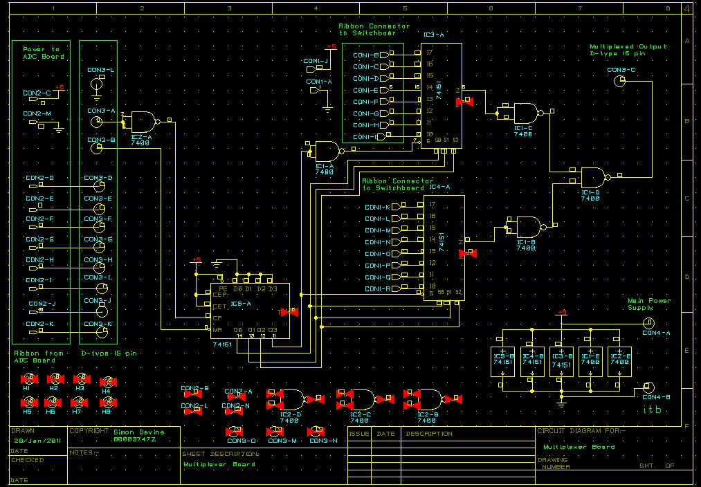
Picture of my schematic

For the first two weeks I had to transfer a schematic of a multiplexer board to my own schematic on the PC using CADSTAR software. I then had to transfer my schematic to a PCB schematic. This is also done using CADSTAR as a virtual board. I placed each individual IC were I thought would be appropriate positions. I also had to take into account that another PCB board will be placed above this one, so I tried to avoid placing any ICs underneath were this board would be placed. This was made easier by having the dimensions of each board and were the second board will need to be placed.

Picture of my PCB schematic

Following this, I now had to virtually wire all the components. This was long and tedious as I was trying to separate the wiring and leave sufficient gaps as to not overlap or have problems drilling the PCB later.
After this was completed, I then mitred the PCB to tidy up the wiring. After mitre I rechecked the board, altering any wiring I felt was to close to each other.
I am now ready to print these schematics and prepare for designing the actual PCB board.