 |
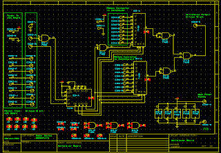
| Picture of my schematic |
For the first two weeks I had to transfer a schematic of a multiplexer board to my own schematic on the PC using CADSTAR software. I then had to transfer my schematic to a PCB schematic. This is also done using CADSTAR as a virtual board. I placed each individual IC were I thought would be appropriate positions. I also had to take into account that another PCB board will be placed above this one, so I tried to avoid placing any ICs underneath were this board would be placed. This was made easier by having the dimensions of each board and were the second board will need to be placed.
 |
| Picture of my PCB schematic |
Following this, I now had to virtually wire all the components. This was long and tedious as I was trying to separate the wiring and leave sufficient gaps as to not overlap or have problems drilling the PCB later.
After this was completed, I then mitred the PCB to tidy up the wiring. After mitre I rechecked the board, altering any wiring I felt was to close to each other.
I am now ready to print these schematics and prepare for designing the actual PCB board.
No comments:
Post a Comment