 |
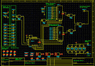
| Multiplexer PCB design print out, front and back |
Having completed the PCB design for the multiplexer using CADstar software last week, I've printed out the design onto translucent paper in order to transfer the design onto PCB board. To transfer the design onto the PCB, the translucent paper was placed over both sides of the PCB and placed into a UV machine for 3 minutes. It's then placed into several tanks containing chemicals to etch out the design onto the PCB.
The tanks are as follows:
Using the tanks I encountered some problems. In the developing tank which uses an acid, it's recommend to leave the PCB board in it for 10-12 second. If you were to leave the PCB in the tank for too long it effects the overall result. Because the chemicals in the tanks were relatively new, the PCB only needed to be in the tank for 5-6 seconds. I had left mine in for 8. After examining the board, although the results were not great, I considered them ok to proceed.
 |
| Outcome of the bottom of the PCB |
The next problem I then encountered was with the etching tank. This strips away all the excess copper from the PCB. Again, if you leave it in for too long it can strip away too much. The problem I had is that it seemed to strip away at one side quicker than the other. I tried to solve this problem by rotating the board, causing this proceedure to take up to 20 to 25 minutes to complete. Nearly ten minutes more than the recommended time. Once again, I examined the board and considered it okay to proceed to the next stage.
The final two tanks were straight forward and caused me no problems. The final outcome of the PCB seemed to be relatively alright. I could trace all the circuitry lines, although they were thin at some points, there were no gaps. The only problems I could see on the board was that the outline of the drill holes were very vague. But this shouldn't be a problem if I just take my time and great care when it comes to drilling the board. I still had the design on paper and could easily mark out the holes to be drilled using a pencil.
The next step in this project is to design an ADC board that will eventually be attached above this board. This will be done similiarly to how the multiplexer PCB design was done.


